Research - Devices

Atomically thin semiconductors: An emerging platform for ultra-low power electronicsThe carbon footprint (~4% of total CO2 emission) of modern electronics is comparable to that of aviation and is expected to rapidly increase due to the rise of artificial intelligence and data-centric approaches such as deep learning that are expected to consume a vast amount of energy. The proposed research aims to engineer the next generation of ultra-low power and energy efficient electronics. The programme is underpinned by our group’s recent breakthroughs in ultra-clean electrical contacts (Nature, 2019 & 2022) on atomically thin semiconductors, realisation of ultra-thin ferroelectric semiconductors (Science, 2022) and demonstration of large area single crystal hexagonal boron nitride as a universal dielectric layer for next generation of electronics (Nature, 2022), which provide the fundamental launching pad for technological innovation. These discoveries allow the realisation of new energy efficient electronic devices that consume very little power and are in principle compatible with the existing electronics infrastructure. |
Ongoing Projects |
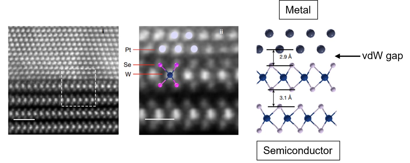
1. Ideal metal/semiconductor interfacesMetal/semiconductor junctions are at the heart of electronics. In this project, we seek to understand the properties of metal contacts on atomically thin semiconductors. To this end, we use van der Waals contacts to realise ultra-clean contacts of atomically thin transition metal dichalcogenide semiconductors. Examples of our work are (Nature 2019 and Nature 2022).
Figure 1. Atomic resolution imaging and schematic of vdW gap at metal/semiconductor interface. (Nature 2022, 568, 70–74). |
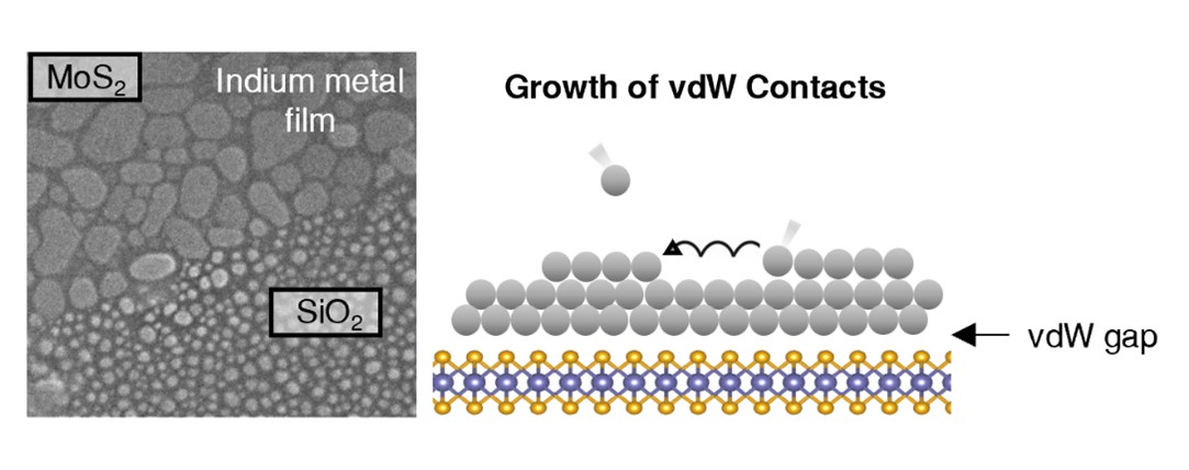
2. Understanding metal deposition on atomically thin semiconductorsElectronic devices based on two-dimensional (2D) materials need ultraclean and defect-free van der Waals (vdW) contacts with three-dimensional (3D) metals. It is therefore important to understand how vdW metal films deposit on 2D surfaces. Our research studies the growth and nucleation of vdW metal films and non-vdW metal films deposited on different 2D materials.
Figure 2. SEM image of In film deposited on monolayer MoS2 and schematic describing the growth of vdW metal thin film. ( ACS Appl. Mater. Interfaces 2024, 16, 6, 7399–7405). |
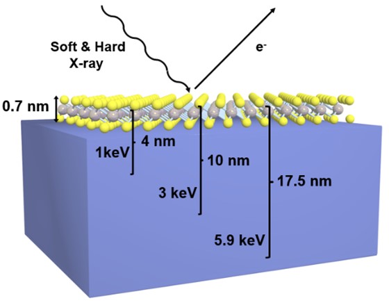
3. Ideal dielectric/semiconductor interfacesZrO2 – a CMOS compatible high κ dielectric – is an ideal substrate for MoS2 because it does not dope or influence the atomically thin semiconductor. The ultra-clean ZrO2/MoS2 interface leads to highly reproducible N-type FETs that operate in enhancement mode with small positive threshold voltages, exhibit very low SS, and high ON state currents.
Figure 3. Schematic of the photoelectron setup, illustrating the probing depths for SiO2. The depth profiling analysis investigates band bending and the associated doping effects at the dielectric/semiconductor interface. |
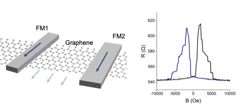
4. Spin valves (LSVs) using ferromagnetic van der Waals contactsWe investigate whether the vacuum gap between graphene and van der Waals metal contact can be used as tunnel barrier for spin injection and collection. We study graphene lateral spin valves (LSVs) using ferromagnetic (FM) vdW contacts of indium and cobalt (In/Co) that does not require deposition of dielectric tunnel barriers.
Figure 4. A representative graphene lateral spin valve with ferromagnetic van der Waals contacts. |
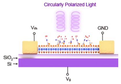
5. Chirality induction in atomically thin semiconductorsWe use chiral molecules to functionalise atomically thin transition metal dichalcogenides to induce chirality and sensitive optoelectronic response to distinguish polarization states of photons. Chirality induction in two dimensional semiconductors leads to interesting and unexpected phenomena.
Figure 5. Detection of left-and right-circularly polarized light with chiral molecule functionalized monolayer MoS2. |
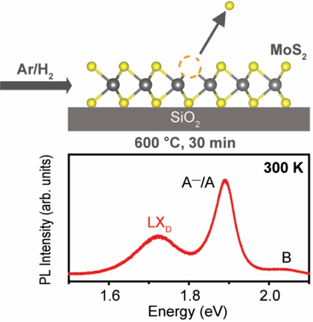
6. Point defects in 2D transition metal dichalcogenidesOur research investigates how monolayer TMDs are influenced by vacancy defects by probing excitonic and defect-mediated PL emission. We find it is possible to observe PL from sulfur vacancies in monolayer MoS2 at room temperature which is typically observed only at low temperatures (≤77 K). The binding energy of excitons trapped at sulfur vacancies is ~185 meV. The sulfur vacancies can be passivated by annealing the sulfur-deficient MoS2 in sulfur vapor, where we observe the suppression of PL from sulfur vacancies. (ACS Nano 2023, 17, 14, 13545–13553).
Figure 6. Generation of sulfur vacancies in monolayer MoS2 by annealing in an Ar/H2 (95%/5%) atmosphere. (ACS Nano 2023, 17, 14, 13545–13553). |
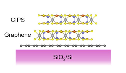
7. Non-volatile memory devices based on CuInP2S6 and graphene vdW heterostructuresWe investigate devices such as ferroelectric FETs and ferroelectric diodes based on CIPS and graphene vdW heterostructures. We study the role of interfaces and influence of polarization in CIPS on tunnelling on transport through graphene.
Figure 7. Schematic of a CIPS/graphene vdW heterostructure on a SiO2/Si substrates. |
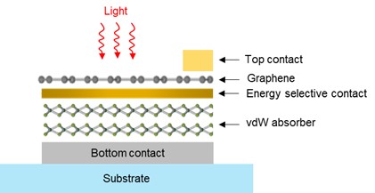
8. van der Waals 2D photovoltaicsOur research focuses on the design, fabrication and characterization of 2D vdW heterostructure-based hot carrier solar cells. We aim to engineer energy selective contact to minimize thermalization loss channels, resulting in high open circuit voltage. We utilise ideal vdW contacts at the metal-semiconductor interface, leading to the low contact resistance and high carrier mobility.
Figure 8. Device strategy for hot carrier extraction in a vertical photovoltaic cell. |