
Publications
2026 | |
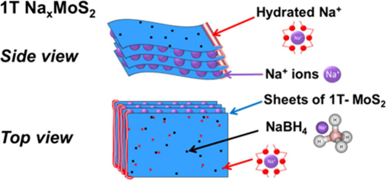 Metallic 1T NaxMoS2 as Sulfur Host for Room Temperature Na–S BatteriesSodium intercalation in layered materials is important for beyond lithium ion-based energy storage technologies. We show that the intercalation of sodium ions using a solid-state reaction between layered molybdenum disulfide (MoS2) and sodium borohydride (NaBH4) at 300 °C in an argon atmosphere leads to a transformation from the semiconducting to metallic phase and the formation of sodium-intercalated MoS2 (NaxMoS2). However, the removal of borohydride by washing with water also dissolves the intercalated Na ions, resulting in nonsodiated 1T phase MoS2. Therefore, 1T phase NaxMoS2 has been difficult to isolate and thus has remained largely unexplored. Here, we show that sequential washing with dimethylformamide (DMF) leads to the effective removal of borohydride while retaining intercalated sodium ions. This process yields stabilized NaxMoS2 (x ≈ 0.6 as determined by electrochemical deposition) with a 1T phase concentration of ∼60% measured by X-ray photoelectron spectroscopy (XPS). High resolution transmission electron microscopy (HR-TEM) results show that the 1T phase is uniformly distributed within the flake. 23Na magic-angle-spinning solid-state nuclear magnetic resonance (23Na ssNMR) confirms the interlayer intercalation of sodium ions. Finally, we employ 1T NaxMoS2 as a sulfur host in Na–S batteries. Cathodes based on 1T NaxMoS2 deliver higher specific capacity and improved cycling stability compared to conventional carbon/sulfur cathodes. These results suggest that 1T NaxMoS2 is promising for room temperature Na–S batteries. | |
E. Gray et al. ● 20/05/2026 ● ACS Nano | |
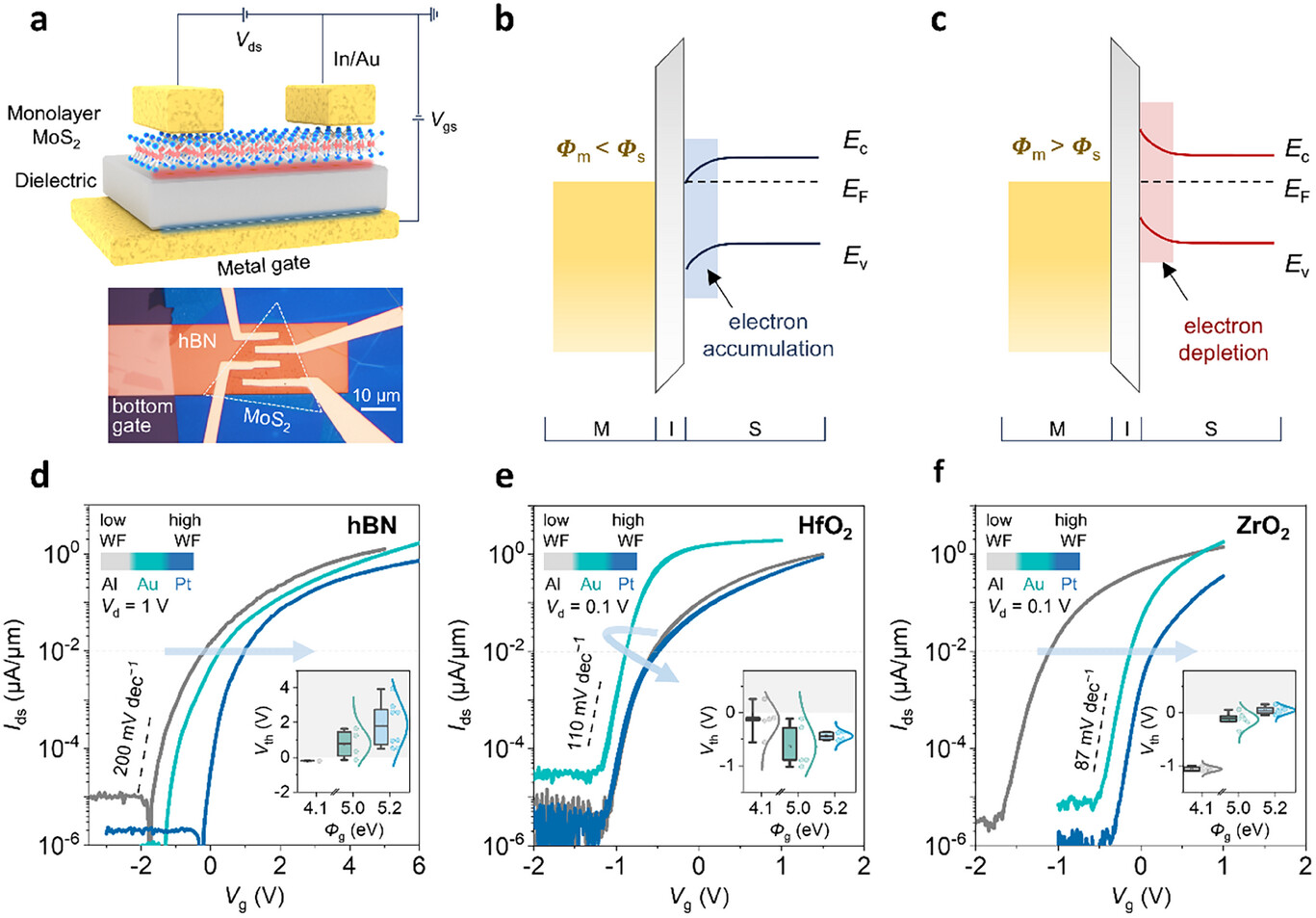 Dielectric and Gate Metal Engineering for Threshold Voltage Modulation in Enhancement Mode Monolayer MoS2 Field Effect TransistorsExcellent gate electrostatics in field effect transistors (FETs) based on 2D transition metal dichalcogenide (2D TMD) channels can dramatically decrease static power dissipation. Energy-efficient FETs operate in enhancement mode with a small and positive threshold voltage (Vth) for n-type devices. However, most state-of-the-art FETs based on monolayer MoS2 channel operate in depletion mode with negative Vth due to doping from the underlying dielectric substrate. In this work, we identify key properties of the semiconductor/dielectric interface (MoS2 on industrially relevant high dielectric constant (k) HfO2, ZrO2 and hBN for reference) responsible for realizing enhancement-mode operation of 2D MoS2 channel FETs. We find that hBN and ZrO2 dielectric substrates provide low defect interfaces with MoS2 that enables effective modulation of the Vthusing gate metals of different work functions (WFs). We use photoluminescence (PL) and synchrotron X-ray photoelectron spectroscopy (XPS)... | |
L. Liu et al. ● 17/03/2026 ● Advanced Materials | |
 Exploring the current engineering challenges of solid‑state lithium‑sulfur batteries with fundamental materials science: A reviewLithium sulfur batteries offer high theoretical energy density and low material cost, but their practical use depends on electrolyte systems that satisfy several fundamental criteria. Solid state electrolytes provide a promising route by removing the liquid phase and improving safety. This review outlines the reaction pathways in lithium sulfur cells and the mechanisms of ion transport in solid electrolytes, followed by a generational comparison of major electrolyte classes, including polymers, oxides, sulfides, halides, garnets and composite systems. Four key criteria for solid state electrolyte use in lithium sulfur batteries are then examined: stability with electrodes, polysulfide behaviour, sulfur utilization and mechanical versatility. Existing strategies are evaluated in terms of how effectively they satisfy each requirement. Finally, two solid state cell designs that meet all identified criteria are proposed, together with quantitative considerations for electrolyte and cathode design. These insights provide a framework for guiding the development of practical solid state lithium sulfur batteries.
| |
Wong, J.Y.A. et al. ● 12/02/2026 ● MRS Energy & Sustainability | |
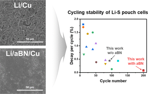
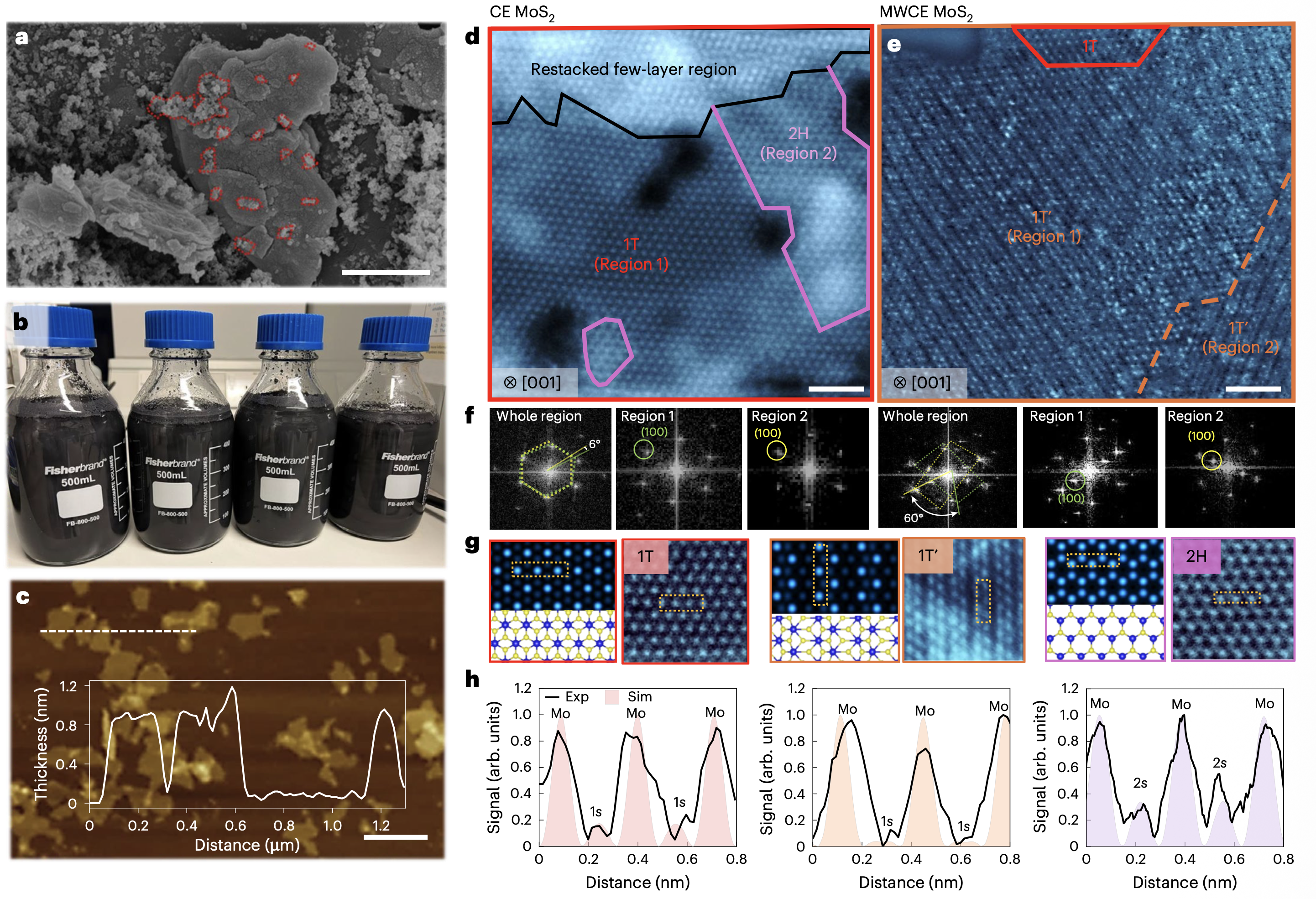 Scalable manufacture of nearly pure-phase metallic MoS2 nanosheetsMetallic, two-dimensional molybdenum disulfide (MoS2) nanosheets show promise for energy storage and catalysis applications. However, current chemical exfoliation methods require more than 48 h to produce milligrams of material, and result in an impure mixture of metallic (1T/1T′, approximately 50%–70%) and semiconducting (2H) phases. Here we demonstrate large-scale and rapid (>600 g h−1) production of nearly pure-phase metallic two-dimensional MoS2 nanosheets using microwave irradiation. Atomic-resolution imaging and X-ray photoelectron spectroscopy show nearly 100% metallic phase in the basal plane. This high purity leads to a large exchange current density (0.175 ± 0.030 mA cm−2) and low Tafel slopes (39–47 mV dec−1) for hydrogen evolution reaction. In supercapacitors and lithium–sulfur pouch-cell batteries, the resulting nanosheets enable a high volumetric capacitance of 753.0 ± 3.6 F cm−3 and a specific capacity of 1,245 ± 16 mAh g−1 (electrolyte-to-sulfur ratio, 2 µl mg−1), respectively. Our method provides a practical pathway for producing high-quality metallic two-dimensional materials for high-performance energy devices. | |
Yang, Z.J et al. ● 04/01/2026 ● Nature Materials | |
2025 | |
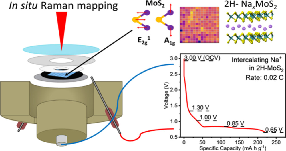 In Situ Raman Mapping of Electrochemical Sodium Intercalation and Phase Stability in MoS2 for Sodium-Ion Batteries
Understanding phase transformations in layered materials such as transition metal dichalcogenides during ion intercalation is critical for developing advanced battery electrodes. Given that the electrochemical behavior of molybdenum disulfide (MoS2) is fundamentally governed by its nanoscale layered structure, understanding its phase stability during sodium-ion (Na+) intercalation is essential for optimizing MoS2 as an anode material for next-generation sodium-ion batteries. In this study, we investigate Na+intercalation into MoS2 and its effect on structural phase evolution by using in situ Raman spectroscopy and ex situ X-ray photoelectron spectroscopy (XPS)... | |
E. Gray et al. ● 29/12/2025 ● ACS Applied Nano Materials | |
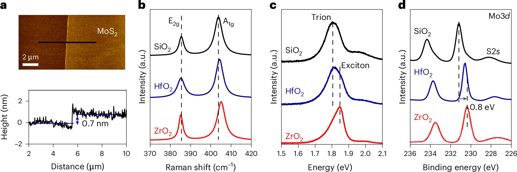 A clean van der Waals interface between the high-k dielectric zirconium oxide and two-dimensional molybdenum disulfideTwo-dimensional transition metal dichalcogenide semiconductors possess ideal attributes for meeting industry scaling targets for transistor channel technology. However, the development of scaled field-effect transistors (FETs) requires industry-compatible gate dielectrics with low equivalent oxide thicknesses. Here we show that zirconium oxide (ZrO2)—an industry-compatible high-dielectric-constant (k) oxide—can form a clean interface with two-dimensional molybdenum disulfide (MoS2). Photoelectron spectroscopy analysis shows that although silicon dioxide and hafnium oxide substrates introduce the doping of MoS2, ZrO2 exhibits no measurable interactions with MoS2. Back-gated monolayer MoS2 FETs... | |
H. Yan et al. ● 06/10/2025 ● Nature Electronics | |
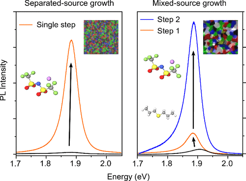 Dual-Step Chemical Treatment of Wafer-Scale Metal–Organic Chemical Vapor Deposition Grown Monolayer Molybdenum DisulfidesTwo-dimensional (2D) transition metal dichalcogenides (TMDs) possess distinct optical and electronic properties, making them promising candidates for optoelectronic applications. Recently, major advances in the wafer-scale growth of TMDs using the metal–organic chemical vapor deposition (MOCVD) have enabled their integration with standard electronics. However, such materials continue to suffer from defects and unwanted doping, which lower semiconductor performance, as exemplified by poor photoluminescence (PL) yield. Chemical treatment protocols have been shown to improve the PL yield in exfoliated and CVD-grown materials. Here, using PL, Raman microscopy, X-ray photoemission spectroscopy (XPS) and density functional theory (DFT) calculations, we develop chemical treatment protocols for wafer-scale MOCVD-grown monolayer MoS2. The postgrowth treatment uses sulfide and TFSI-based ionic salts... | |
J. Lim et al. ● 25/09/2025 ● ACS Publications | |
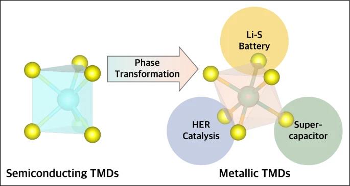 Metallic-phase two-dimensional transition-metal dichalcogenides for electrochemical applicationsIn 2011, we reported facile synthesis of metallic-phase two-dimensional transition-metal dichalcogenide (TMD) nanosheets. This method allows access to metallic materials that are atomically thin and therefore possess properties that are fundamentally different from their bulk counterparts. Since then, thousands of papers have reported synthesis and new applications of metallic atomically thin nanosheets. Over the past 15 years, metallic TMD nanosheets have emerged as leading materials for electrochemical applications in catalysis, supercapacitors, and lithium–sulfur batteries... | |
Z. Yang et al. ● 24/09/2025 ● MRS Bulletin | |
Clean transfer of two-dimensional materials using UV-ozone treated polydimethylsiloxaneThe clean and reliable transfer of two-dimensional (2D) materials is critical for preserving their intrinsic properties and enabling high-performance device applications. This study presents a method utilising UV-ozone treated polydimethylsiloxane (UV-PDMS) as a transfer medium to achieve residue-free 2D materials. The UV-PDMS transfer method increases surface rigidity, reduces surface polymeric residues, and ensures intimate contact between 2D materials... | |
H. Yan et al. ● 12/09/2025 ● 2D Materials | |
 Ultrathin Amorphous Boron Nitride Films and Their Functional Integration in Lithium Metal AnodesUltrathin amorphous materials are promising counterparts to 2D crystalline materials, yet their properties and functionalities remain poorly understood. Amorphous boron nitride (aBN) has attracted attention for its ultralow dielectric constant and superior manufacturability compared with hexagonal boron nitride. Here, we demonstrate wafer-scale growth of ultrathin aBN films with exceptional thickness and composition uniformity using capacitively coupled plasma-chemical vapor deposition (CCP-CVD) at 400 °C. Beyond dielectric applications, we reveal an unexpected functionality─serving as an interfacial layer in Li anode current collectors... | |
H. Kim et al. ● 08/09/2025 ● Nano Letters | |
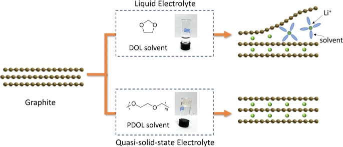 Stabilising graphite anode with quasi-solid-state electrolyte for long-life lithium–sulfur batteriesLithium–sulfur (Li–S) batteries with high energy density are promising for next-generation energy storage but suffer from poor cycle life due to instability of the lithium anode. Commercial graphite anodes used in lithium-ion batteries could be viable for replacement of lithium metal as anode in Li–S batteries. However, graphite anodes are incompatible with the commonly used ether-based electrolytes in Li–S batteries due to the Li+ ion and solvent co-intercalation into graphite interlayers, which leads to exfoliation. Here, we report the stabilisation of graphite anode by in-situ formation of quasi-solid-state electrolyte (QSSE) in Li–S batteries... | |
Z. Li et al. ● 14/07/2025 ● MRS Energy & Sustainability | |
 Gate dielectrics for transistors based on two-dimensional transition metal dichalcogenide semiconductorsAchieving low-defect interfaces between industry compatible oxide dielectrics and two-dimensional (2D) transition metal dichalcogenide (TMD) semiconducting channels remains challenging but is the key for unlocking their potential for high-performance field-effect transistors (FETs). This perspective analyses the state of the art on 2D TMD and dielectric interfaces, highlighting key challenges in depositing oxide dielectrics on top of atomically thin TMD semiconductors... | |
H. Yan et al. ● 01/07/2025 ● APL Electronic Devices | |
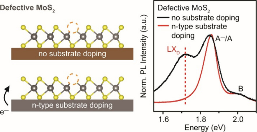 Effect of Substrate on Sulfur Vacancy Defect-Mediated Photoluminescence in Two-Dimensional MoS2Chalcogen vacancy defects in monolayer transition metal dichalcogenides form in-gap states that can trap excitons, leading to defect-mediated photoluminescence (PL) emission. Here, we show that room-temperature (RT, 300 K) PL from sulfur vacancies in defective monolayer MoS2 is sensitive to doping from dielectric substrates such as SiO2 and HfO2. The defect-mediated PL is observed for monolayer MoS2 on untreated HfO2 but is quenched on untreated SiO2... | |
Y. Zhu et al. ● 18/04/2025 ● Journal of Physical Chemistry C | |
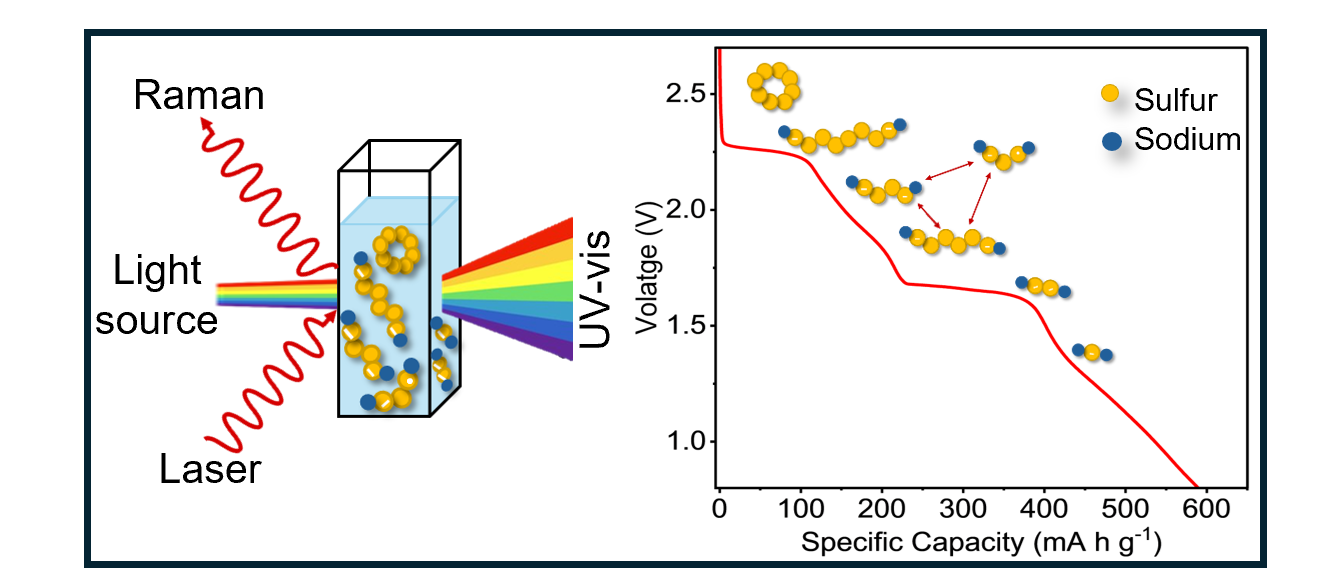 Mapping Polysulfides in Sodium–Sulfur BatteriesSodium–sulfur (Na–S) batteries provide lithium-free alternatives to lithium–sulfur (Li–S) batteries. Na–S chemistry has been less studied. Thus, the types of polysulfides (PS) and their evolution during charge–discharge of Na–S batteries are not as well understood as those in the Li–S system. We, therefore, study the formation of different PS in tetraethylene glycol dimethyl ether-based electrolyte... | |
E. Gray et al. ● 28/02/2025 ● ACS Nano | |
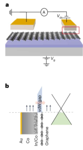 Spin injection in graphene using ferromagnetic van der Waals contacts of indium and cobaltGraphene-based spintronic devices require efficient spin injection, and dielectric tunnel barriers are typically used to facilitate spin injection. However, the direct growth of ultrathin dielectrics on two-dimensional surfaces is challenging and unreliable. Here we report spin injection in graphene lateral spin valves using ferromagnetic van der Waals contacts of indium and cobalt (In–Co), and without the deposition of dielectric tunnel barriers.... | |
S. Sarkar et al. ● 20/01/2025 ● Nature Electronics | |
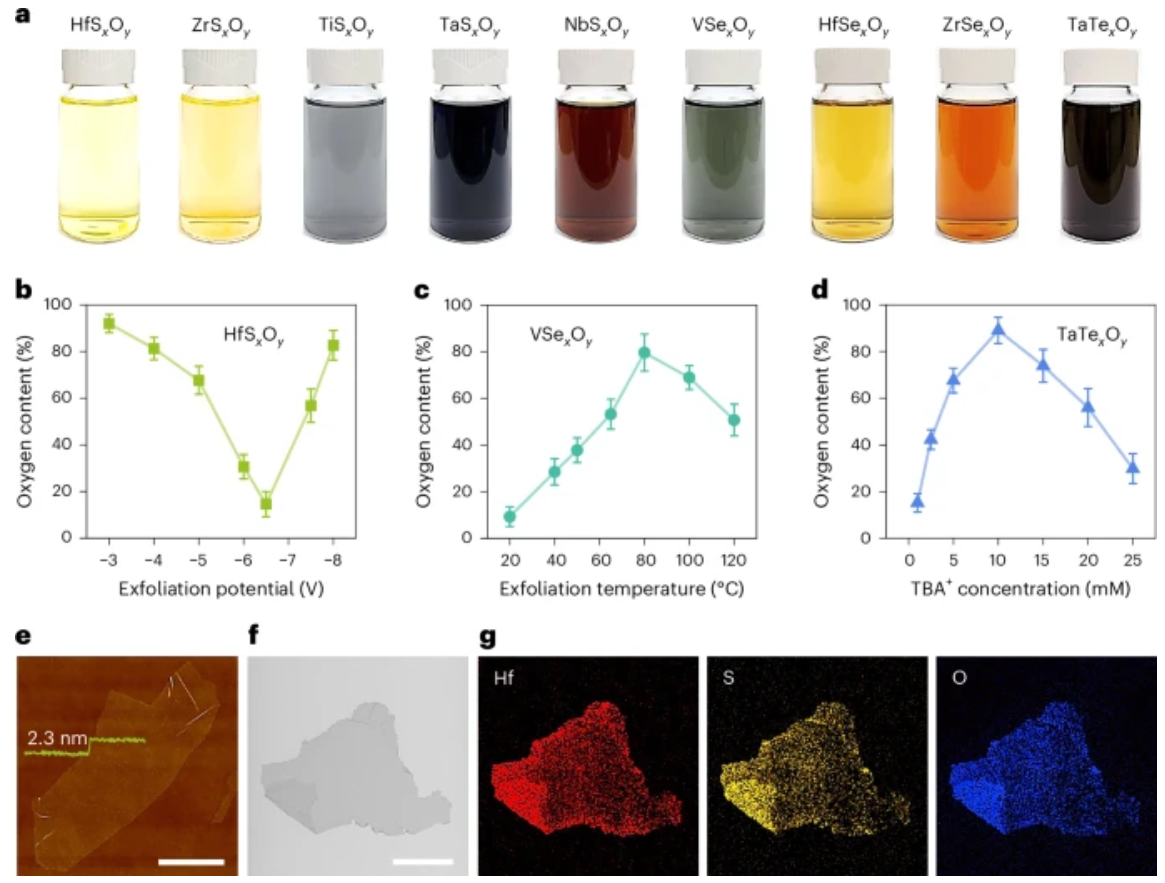 Ultrathin transition metal oxychalcogenide catalysts for oxygen evolution in acidic mediaTwo-dimensional transition metal dichalcogenides (TMDs) exfoliated from bulk layered materials possess interesting properties. Most transition metal oxides are not layered and therefore cannot be exfoliated. Here we report the synthesis of a family of ultrathin materials—transition metal oxychalcogenides (TMOCs)—and demonstrate their unique properties. Two-dimensional TMOCs (MXxOy, M = group IV or V transition metal, X = chalcogen, O = oxygen; x, y = 0–2) from bulk transition metal dichalcogenides (MX2) have been fabricated using tetrabutylammonium .... | |
W. Xu et al. ● 02/01/2025 ● Nature Synthesis | |
2024 | |
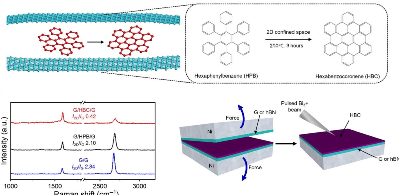 Pressure enabled organic reactions via confinement between layers of 2D materialsConfinement of reactants within nanoscale spaces of low-dimensional materials has been shown to provide reorientation of strained reactants or stabilization of unstable reactants for synthesis of molecules and tuning of chemical reactivity. While few studies have reported chemistry within zero-dimensional pores and one-dimensional nanotubes, organic reactions in confined spaces between two-dimensional materials have yet to be explored. Here, we demonstrate that reactants confined between atomically thin sheets of graphene or hexagonal boron nitride experience pressures as high as 7 gigapascal, which allows the propagation of solvent-free organic reactions that ordinarily do not occur under standard conditions.... | |
S. I. Yoon et al. ● 08/11/2024 ● Science Advances | |
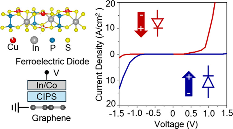 Multistate Ferroelectric Diodes with High Electroresistance Based on van der Waals HeterostructuresSome van der Waals (vdW) materials exhibit ferroelectricity, making them promising for novel nonvolatile memories (NVMs) such as ferroelectric diodes (FeDs). CuInP2S6 (CIPS) is a well-known vdW ferroelectric that has been integrated with graphene for memory devices. Here we demonstrate FeDs with self-rectifying, hysteretic current–voltage characteristics based on vertical heterostructures of 10 nm thick CIPS and graphene. By using vdW indium–cobalt top electrodes and graphene bottom electrodes, we achieve a high electroresistance (on- and off-state resistance ratios) of ∼106, an on-state rectification ratio of 2500 for read/write voltages of 2 V/0.5 V, and a maximum output current density of 100 A/cm2. These metrics compare favorably with state-of-the-art FeDs. Piezoresponse force... | |
S. Sarkar et al. ● 09/10/2024 ● Nano Letters | |
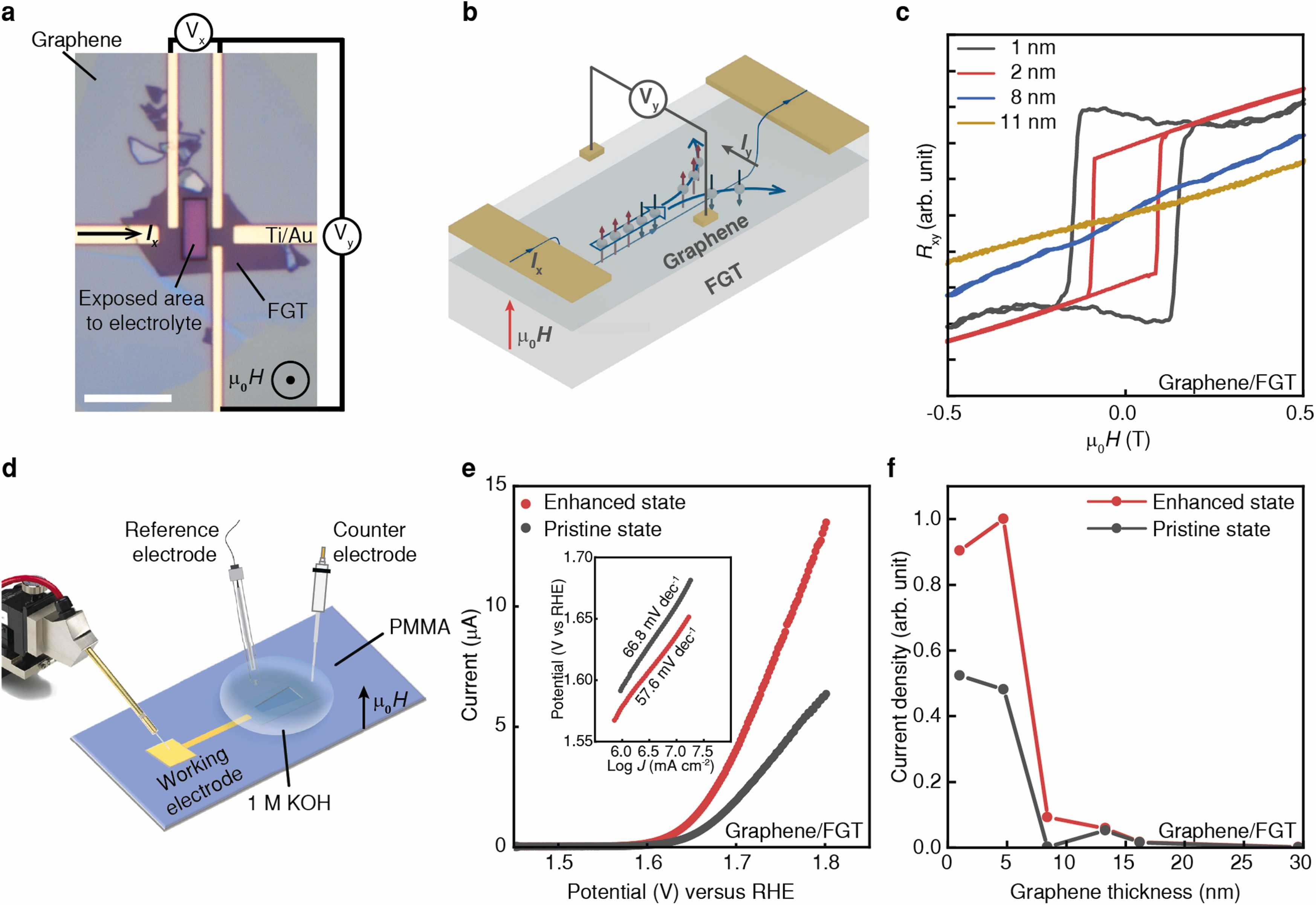 Spin-dependent electron transfer in electrochemically transparent van der Waals heterostructures for oxygen evolution reactionSpin selective catalysis is an emerging approach for improving the thermodynamics and kinetics of reactions. The role of electron spins has been scarcely studied in catalytic reactions. One exception is the oxygen evolution reaction (OER) where strongly correlated metals and oxides are used as catalysts. In OER, spin alignment facilitates the transition of singlet state of the reactant to the triplet state of O2. However, the influence of strong correlations on spin exchange mechanism and spin selective thermodynamics of most catalytic reactions remain unclear. Here we decouple the strongly correlated catalyst from the electrolyte to study spin exchange in two-dimensional (2D) magnetic iron germanium telluride (FGT)... | |
Y. Li et al. ● 19/09/2024 ● Materials Science and Engineering: R: Reports | |
 Broad Adaptability of Coronavirus Adhesion Revealed from the Complementary Surface Affinity of Membrane and SpikesCoronavirus stands for a large family of viruses characterized by protruding spikes surrounding a lipidic membrane adorned with proteins. The present study explores the adhesion of transmissible gastroenteritis coronavirus (TGEV) particles on a variety of reference solid surfaces that emulate typical virus-surface interactions. Atomic force microscopy informs about trapping effectivity and the shape of the virus envelope on each surface, revealing that the deformation of TGEV particles spans from 20% to 50% in diameter. Given this large deformation range... | |
A. B. García-Arribas et al. ● 04/09/2024 ● Advanced Science | |
 Mapping lithium–sulfur chemistryLithium–sulfur batteries are based on complex chemical reactions involving solid–liquid–solid phase transitions. Now, a ternary diagram that describes the thermodynamic stability of the different phases formed during lithium–sulfur reactions is established... | |
Z. Li et al. ● 02/09/2024 ● Nature Chemical Engineering | |
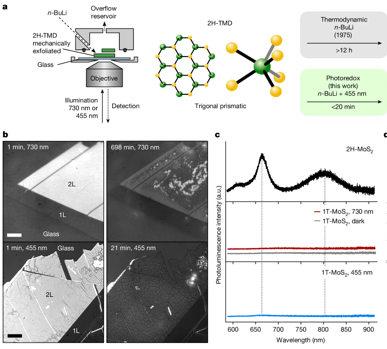 Photoredox phase engineering of transition metal dichalcogenidesCrystallographic phase engineering plays an important part in the precise control of the physical and electronic properties of materials. In two-dimensional transition metal dichalcogenides (2D TMDs), phase engineering using chemical lithiation with the organometallization agent n-butyllithium (n-BuLi), to convert the semiconducting 2H (trigonal) to the metallic 1T (octahedral) phase, has been widely explored for applications in areas such as transistors, catalysis and batteries. Although this chemical phase engineering can be performed at ambient temperatures and pressures, the underlying mechanisms are poorly understood, and the use of n-BuLi raises notable safety concerns. Here we optically visualize the archetypical phase transition from the 2H to the 1T phase in mono- and bilayer 2D TMDs and discover that this reaction can be accelerated by up to six orders of magnitude using low-power illumination at 455 nm... | |
J. Lim et al. ● 28/08/2024 ● Nature | |
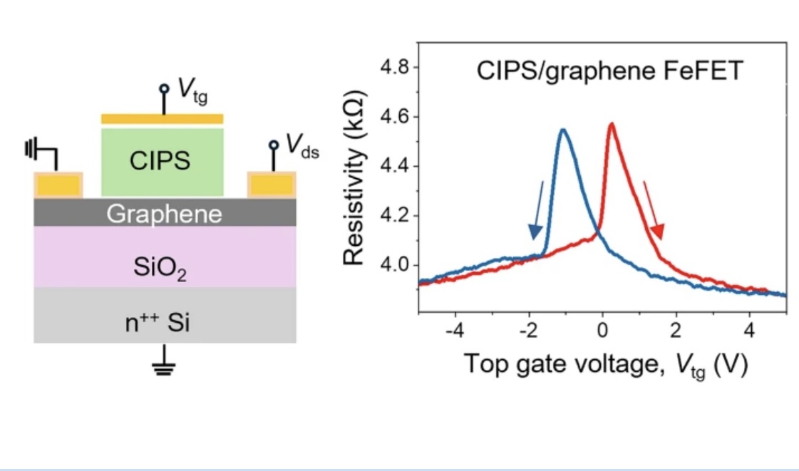 Ferroelectric field effect transistors based on two-dimensional CuInP2S6 (CIPS) and graphene heterostructuresHeterostructures of two-dimensional (2D) materials comprise clean van der Waals (vdW) interfaces that can facilitate charge or energy transfer. Recently, the 2D ferroelectric CuInP2S6 (CIPS) has been integrated with graphene and other 2D materials to realize potentially novel low energy electronic devices. However, the influence of 2D CIPS on the properties of graphene and doping across the vdW interface has not been studied in detail. Here, we study graphene field effect transistors (FETs) with CIPS as the top gate... | |
M. A. Ghani et al. ● 21/08/2024 ● MRS Energy and Sustainability | |
 Critical challenges in the development of electronics based on two-dimensional transition metal dichalcogenidesThe development of high-performance electronic devices based on two-dimensional (2D) transition metal dichalcogenide semiconductors has recently advanced from one-off proof-of-principle demonstrations to more reproducible integrated devices. It has, in particular, reached a point where the material quality—as well as the interfaces between the metal contacts, dielectrics and 2D semiconductors—must be optimized to increase device performance. Here we examine the key immediate challenges for the development... | |
Y. Wang et al. ● 29/07/2024 ● Nature Electronics | |
 Scanning Plasmon-Enhanced Microscopy for Simultaneous Optoelectrical CharacterizationScanning microscopy methods are crucial for the advancement of nanoelectronics. However, the vertical nanoprobes in such techniques suffer limitations such as the fragility at the tip–sample interface, complex instrumentation, and the lack of in operando functionality in several cases. Here, we introduce scanning plasmon-enhanced microscopy (SPEM) and demonstrate its capabilities on MoS2 and WSe2 nanosheets. SPEM combines a nanoparticle-on-mirror (NPoM)... | |
J. Symonowicz et al. ● 27/07/2024 ● ACS Nano | |
 Recent Advances on Carbon-Based Metal-Free Electrocatalysts for Energy and Chemical ConversionsOver the last decade, carbon-based metal-free electrocatalysts (C-MFECs) have become important in electrocatalysis. This field is started thanks to the initial discovery that nitrogen atom doped carbon can function as a metal-free electrode in alkaline fuel cells. A wide variety of metal-free carbon nanomaterials, including 0D carbon dots, 1D carbon nanotubes, 2D graphene, and 3D porous carbons, has demonstrated high electrocatalytic performance across a variety of applications. These include clean energy generation... | |
Q. Zhai et al. ● 25/07/2024 ● Advanced Materials | |
 A New Vision for MRS Energy & SustainabilityProf. Chhowalla's Editorial "A new vision for MRS Energy & Sustainability" has been published online in MRS Energy and Sustainability. | |
M. Chhowalla ● 09/07/2024 ● MRS Energy & Sustainability | |
 Quasi-Solid-State Electrolyte Induced by Metallic MoS2 for Lithium-Sulfur BatteriesMolybdenum disulfide (MoS2) can exist in the semiconducting (2H) or metallic (1T) phase. The metallic 1T phase of MoS2 is achieved by lithium intercalation using n-butyllithium. The resulting 1T MoS2 can be in a lithiated form (LixMoS2) or as pure MoS2. The 1T phase of MoS2 is metastable and relaxes to the stable 2H phase upon heating. Here we study the thermal and environmental stabilities of metallic phase LixMoS2 and pure 1T phase MoS2 for comparison. We find that the thermal stability of 1T MoS2 is enhanced by lithiation so that LixMoS2 is phase stable up to 400 °C in argon... | |
Z. Li et al. ● 04/06/2024 ● ACS Nano | |
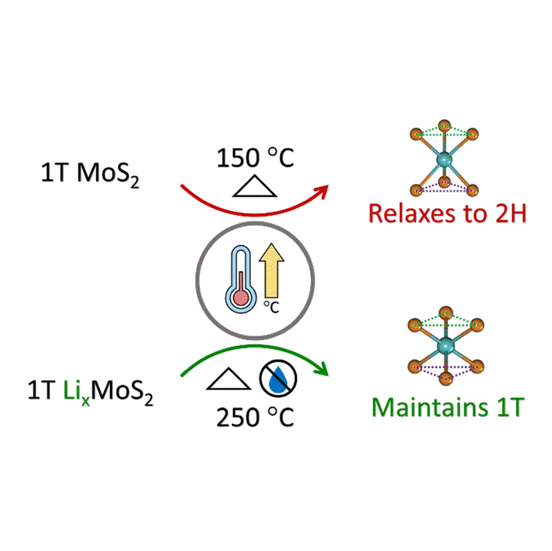 Environmental and Thermal Stability of Chemically Exfoliated LixMoS2 for Lithium–Sulfur BatteriesMolybdenum disulfide (MoS2) can exist in the semiconducting (2H) or metallic (1T) phase. The metallic 1T phase of MoS2 is achieved by lithium intercalation using n-butyllithium. The resulting 1T MoS2 can be in a lithiated form (LixMoS2) or as pure MoS2. The 1T phase of MoS2 is metastable and relaxes to the stable 2H phase upon heating. Here we study the thermal and environmental stabilities of metallic phase LixMoS2 and pure 1T phase MoS2 for comparison. We find that the thermal stability of 1T MoS2 is enhanced by lithiation so that LixMoS2 is phase stable up to 400 °C in argon... | |
Z. J. Yang et al. ● 19/04/2024 ● Chemistry of Materials | |
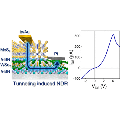 Room Temperature Negative Differential Resistance with High Peak Current in MoS2/WSe2 HeterostructuresTwo-dimensional transition metal dichalcogenide (2D TMD) semiconductors allow facile integration of p- and n-type materials without a lattice mismatch. Here, we demonstrate gate-tunable n- and p-type junctions based on vertical heterostructures of MoS2 and WSe2 using van der Waals (vdW) contacts. The p–n junction shows negative differential resistance (NDR) due to Fowler–Nordheim (F–N) tunneling through the triangular barrier formed by applying a global back-gate bias (VGS). We also show that the integration of hexagonal boron nitride (h-BN) as an insulating tunnel barrier between MoS2 and WSe2 leads to ... | |
J. H. Kim et al. ● 16/02/2024 ● ACS Nano Letters | |
 Metal Films on Two-Dimensional Materials: van der Waals Contacts and Raman Enhancement | |
M. A. Ghani et al. ● 06/02/2024 ● ACS Applied Materials and Interfaces | |
2023 | |
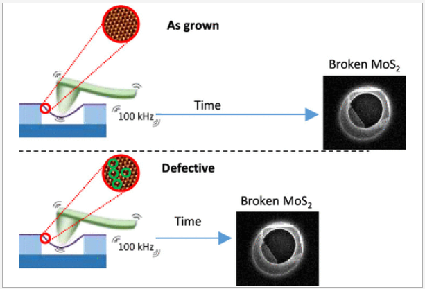 Fatigue Response of MoS2 with Controlled Introduction of Atomic VacanciesFatigue-induced failure resulting from repetitive stress–strain cycles is a critical concern in the development of robust and durable nanoelectromechanical devices founded on 2D semiconductors. Defects, such as vacancies and grain boundaries, inherent in scalable materials can act as stress concentrators and accelerate fatigue fracture. Here, we investigate MoS2 with controlled atomic ... | |
Y. Manzanares-Negro et al. ● 16/11/2023 ● ACS Nano Lett. | |
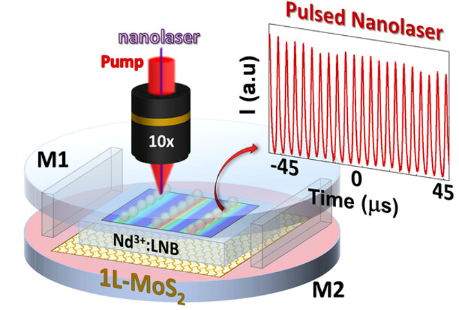 Integrating 2D Materials and Plasmonics on Lithium Niobate Platforms for Pulsed Laser Operation at the NanoscaleThe current need for coherent light sources for integrated (nano)photonics motivates the search for novel laser designs emitting at technologically relevant wavelengths with high-frequency stability and low ... | |
M. O. Ramírez et al. ● 08/11/2023 ● Laser & Photonics Rev. | |
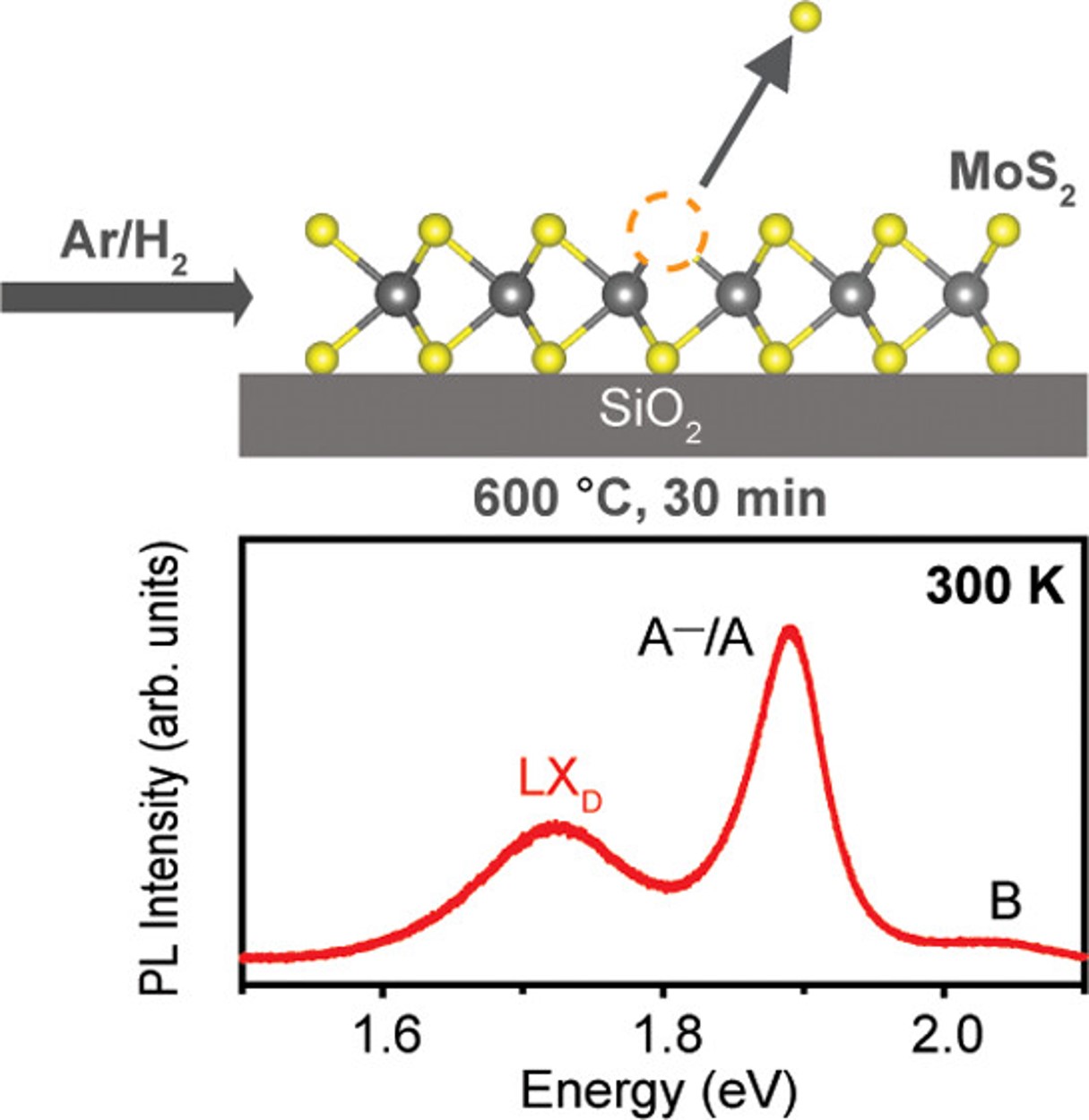 Room-Temperature Photoluminescence Mediated by Sulfur Vacancies in 2D Molybdenum DisulfideAtomic defects in monolayer transition metal dichalcogenides (TMDs) such as chalcogen vacancies significantly affect their properties. In this work, we provide a reproducible and facile strategy to rationally induce chalcogen vacancies in monolayer MoS2 by annealing at 600 °C in an argon/hydrogen (95%/5%) atmosphere. Synchrotron X-ray photoelectron spectroscopy shows that a Mo 3d5/2 core peak at 230.1 eV emerges in the annealed MoS2 associated with nonstoichiometric MoSx (0 < x < 2), and Raman … | |
Y. Zhu et al. ● 7/7/2023 ● ACS Nano | |
 Nanoscale Cathodoluminescence and Conductive Mode Scanning Electron Microscopy of van der Waals HeterostructuresBatteries based on redox chemistries that can store more energy than state-of-the-art lithium-ion systems will play an important role in enabling the energy transition to net zero carbon emissions. Lithium–sulfur (Li–S) batteries have shown extraordinary promise, where the electrically insulating sulfur must be loaded onto a conducting host. Here we report the use of pre-lithiated metallic 1T phase two-dimensional (2D) molybdenum disulfide (LixMoS2) as a sulfur host material for high-performance Li–S batteries under ... | |
H. Ramsden et al. ● 15/6/2023 ● ACS Nano | |
 Lithiated metallic molybdenum disulfide nanosheets for high-performance lithium–sulfur batteriesvan der Waals heterostructures (vdW-HSs) integrate dissimilar materials to form complex devices. These rely on the manipulation of charges at multiple interfaces. However, at present, submicrometer variations in strain, doping, or electrical breakages may exist undetected within a device, adversely affecting macroscale performance. Here, we use conductive mode and cathodoluminescence scanning electron microscopy (CM-SEM and SEM-CL) to investigate these phenomena … | |
Z. Li et al. ● 12/1/2023 ● Nature Energy | |
2022 | |
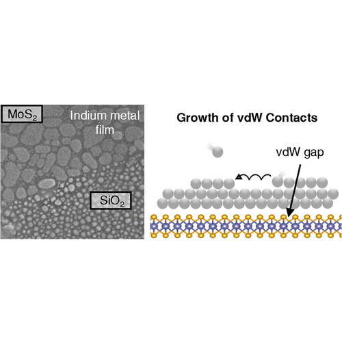
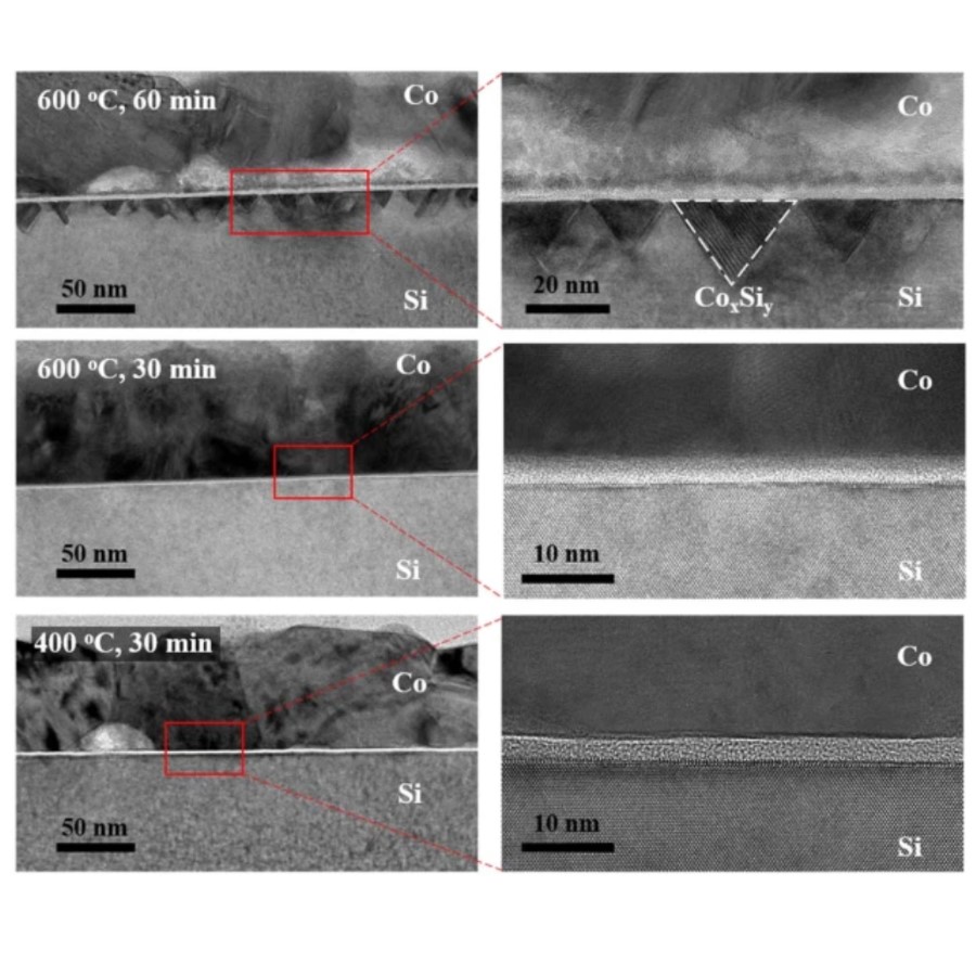
P-type electrical contacts for two-dimensional transition metal dichalcogenidesElectronic devices based on two-dimensional (2D) materials will need ultraclean and defect-free van der Waals (vdW) contacts with three-dimensional (3D) metals. It is therefore important to understand how vdW metal films deposit on 2D surfaces. Here, we study the growth and nucleation of vdW metal films of indium (In) and non-vdW metal films of gold (Au), deposited on 2D MoS2 and graphene. In follows a 2D growth mode in contrast to Au that follows a 3D growth mode. Atomic force microscopy (AFM) and scanning electron microscopy (SEM) were used to image the morphology of metal clusters during growth and quantify the nucleation density... | |
Y. Yang et al. ● 1/8/2022 ● nature | |
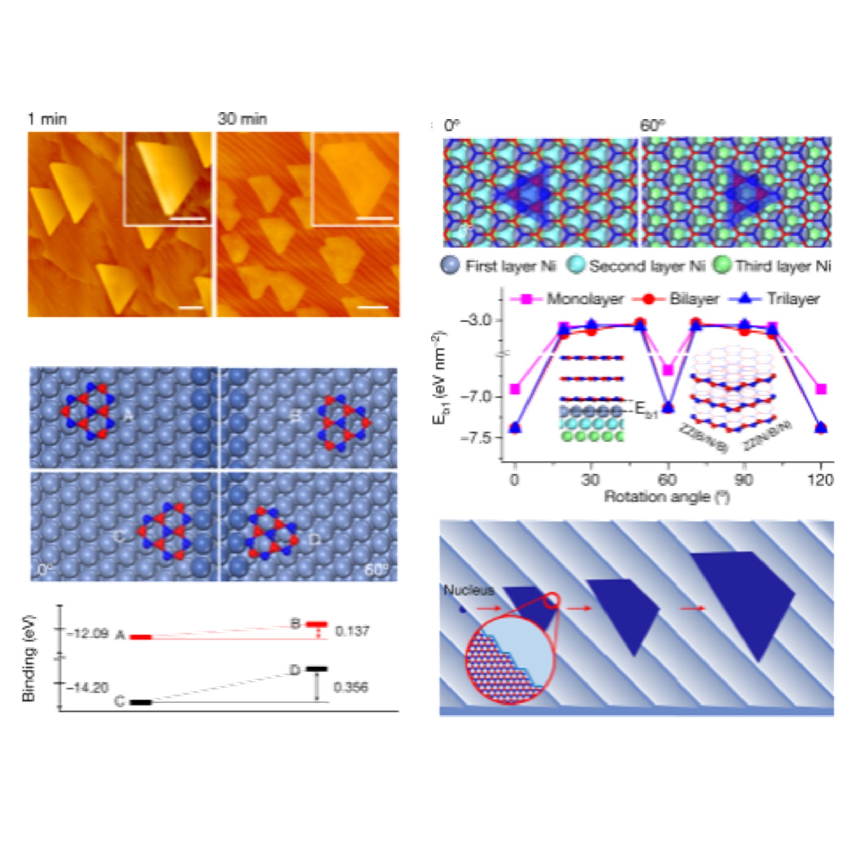 Epitaxial single-crystal hexagonal boron nitride multilayers on Ni (111)Large-area single-crystal monolayers of two-dimensional (2D) materials such as graphene1,2,3, hexagonal boron nitride (hBN)4,5,6 and transition metal dichalcogenides7,8 have been grown. hBN is considered to be the ‘ideal’ dielectric for 2D-materials-based field-effect transistors (FETs), offering the potential for extending Moore’s law9,10. Although hBN thicker than a monolayer is more desirable as substrate for 2D semiconductors11,12, highly uniform and single-crystal multilayer hBN growth ... | |
K. Y. Ma et al. ● 1/6/2022 ● nature | |
| |
 Ferroelectricity in untwisted heterobilayers of transition metal dichalcogenidesTwo-dimensional materials with out-of-plane (OOP) ferroelectric and piezoelectric properties are highly desirable for the realization of ultrathin ferro- and piezoelectronic devices. We demonstrate unexpected OOP ferroelectricity and piezoelectricity in untwisted, commensurate, and epitaxial MoS2/WS2 heterobilayers synthesized by scalable one-step chemical vapor deposition. We show d33 piezoelectric constants of 1.95 to 2.09 picometers per volt that are larger than the natural OOP piezoelectric ... | |
L. Rogee et al. ● 26/5/2022 ● Science | |
| |
 Ultrahigh Pt-Mass-Activity Hydrogen Evolution Catalyst Electrodeposited from Bulk PtMaximizing the Pt utilization is important for the widescale implementation of Pt-based hydrogen evolution reaction (HER) electrocatalysts, owing to the scarcity of Pt. Here, three-component heterostructured HER catalysts with ultrahigh Pt mass activity in which hollow PtCu alloy nanospheres are supported on an array of WO3 on Cu foam, are reported. It has been pointed out that the use of Pt counter electrode in a three-electrode configuration in evaluating catalysts’ HER performances in ... | |
L. Liu et al. ● 18/2/2022 ● Advanced Functional Materials | |
| |
Tanks and Truth | |
N. Kotov et al. ● 22/3/2022 ● ACS Nano | |
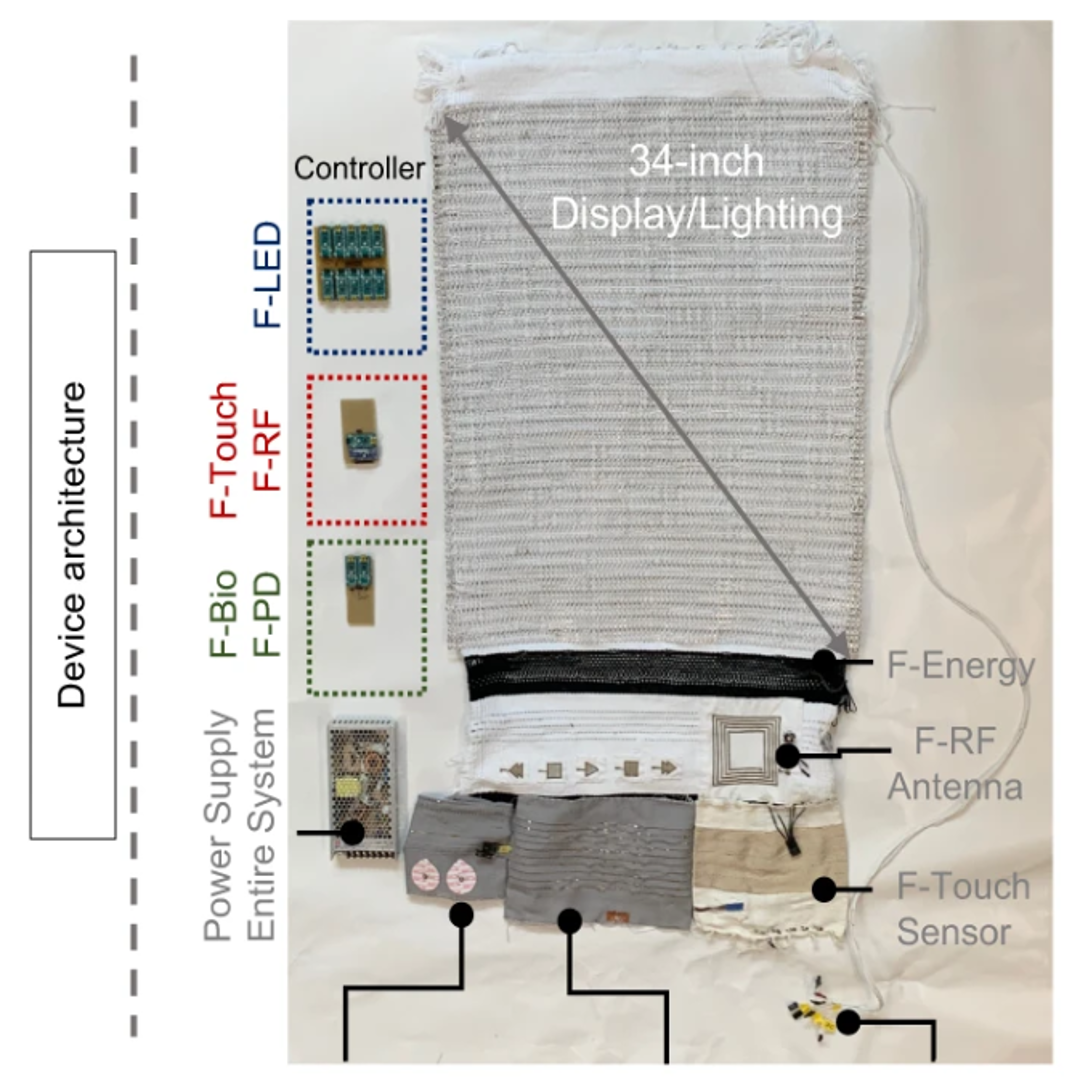 Smart textile lighting/display system with multifunctional fibre devices for large scale smart home and IoT applicationsSmart textiles consist of discrete devices fabricated from—or incorporated onto—fibres. Despite the tremendous progress in smart textiles for lighting/display applications, a large scale approach for a smart display system with integrated multifunctional devices in traditional textile platforms has yet to be demonstrated. Here we report ... | |
H. Choi et al. ● 10/2/2022 ● Nature Communications | |
2021 | |
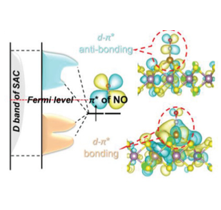 3.4% Solar-to-Ammonia Efficiency from Nitrate Using Fe Single Atomic Catalyst Supported on MoS2 NanosheetsElectrochemical synthesis of NH3 is a carbon-free alternative to the traditional Haber–Bosch process. Obtaining NH3 from environmental pollutants, such as nitrates or nitrites, is a more practical route than from the nitrogen reduction reaction (NRR) due to the difficult cleavage of the inert triple bond of nitrogen gas. Here, a novel heterogeneous catalyst is reported based on iron (Fe) single-atoms supported on 2D MoS2 (Fe-MoS2) for the nitrate reduction reaction (NO3RR). Fe-MoS2 exhibits ... | |
J. Li et al. ● 22/12/2021 ● Advanced Functional Materials | |
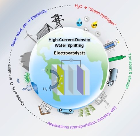 Recent Advances in Design of Electrocatalysts for High‐Current‐Density Water SplittingElectrochemical water splitting technology for producing “green hydrogen” is important for the global mission of carbon neutrality. Electrocatalysts with decent performance at high current densities play a central role in the industrial implementation of this technology. This field has advanced immensely in recent years, as witnessed by many types of catalysts designed and synthesized toward industrially-relevant current densities (> 200 mA cm–2). By discussing recent advances in ... | |
Y. Luo et al. ● 4/12/2021 ● Advanced Materials | |
Making clean electrical contacts on 2D transition metal dichalcogenides2D semiconductors, particularly transition metal dichalcogenides (TMDs), have emerged as highly promising for new electronic technologies. However, a key challenge in fabricating devices out of 2D semiconductors is the need for ultra-clean contacts with resistances approaching the quantum limit. The lack of high-quality, low-contact-resistance P-type and N-type contacts on 2D TMDs has limited progress towards the next generation of low-power devices, such as the tunnel field-effect transistors ... | |
Y. Wang et al. ● 3/12/2021 ● Nature Review Physics, Pages 1-12 | |
Stabilizing Lithium Anode Via Separator Engineering and in-Situ Electrolyte Additive Tuned SEILi metal anode is regarded as one of the rising stars in secondary batteries systems. Safety issues attributing from lithium dendrites, however, greatly hinders its practical application. Here we present an effective and scalable way of protecting lithium metal anode via separator engineering, and further through the tuning of solid electrolyte interface (SEI) via Li+/functional group bonding. The novel separator exhibits much higher specific surface area (~16.9x) and enhanced ionic conductivity (~3.25x) than ... | |
M. Fei et al. ● 10/10/2021 ● The Electrochemical Society Meeting Abstracts, Volume MA2021-02, 1903 | |
 2021 roadmap on lithium sulfur batteriesBatteries that extend performance beyond the intrinsic limits of Li-ion batteries are among the most important developments required to continue the revolution promised by electrochemical devices. Of these next-generation batteries, lithium sulfur (Li–S) chemistry is among the most commercially mature, with cells offering a substantial increase in gravimetric energy density, reduced costs and improved safety prospects. However, there remain outstanding issues to advance ... | |
J. B. Robinson et al. ● 23/3/2021 ● Journal of Physics: Energy, Volume 3, Number 3 | |
 Reply to: On the measured dielectric constant of amorphous boron nitrideIn the accompanying Comment1, Li and Chen state that the dielectric constant (κ) values we reported for amorphous boron nitride (a-BN)2 are underestimated and are inconsistent with principles of dielectric physics. Here we show that the claims of Li and Chen are incorrect, using our original data and new data that support our initial results ... | |
S. Hong et al. ● 3/2/2021 ● Nature, 590, E8-10 | |
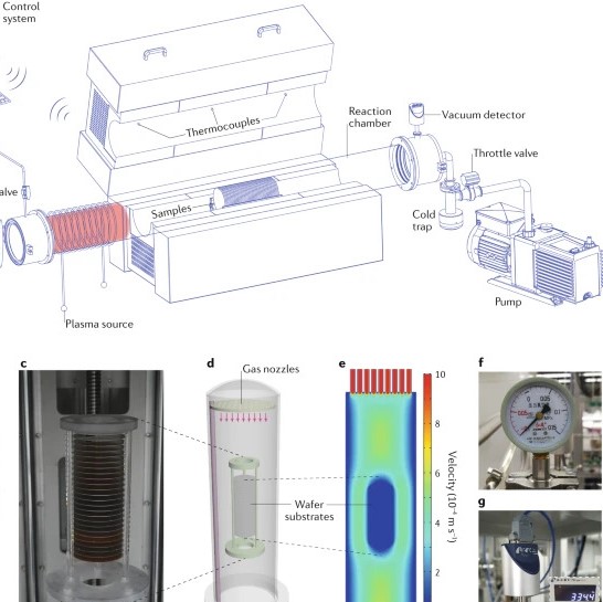 Chemical vapour deposition Chemical vapour deposition (CVD) is a powerful technology for producing high-quality solid thin films and coatings. Although widely used in modern industries, it is continuously being developed as it is adapted to new materials. Today, CVD synthesis is being pushed to new heights with the precise manufacturing of both inorganic thin films of 2D materials and high-purity polymeric ... | |
L. Sun et al. ● 14/1/2021 ● Nature Review Methods Primers, 1, Article Number 5 | |
2020 | |
In Situ Scanning Transmission Electron Microscopy Observations of Fracture at the Atomic Scale The formation, propagation, and structure of nanoscale cracks determine the failure mechanics of engineered materials. Herein, we have captured, with atomic resolution and in real time, unit cell-by-unit cell lattice-trapped cracking in two-dimensional (2D) rhenium disulfide (ReS2) using in situ aberration corrected scanning transmission electron microscopy (STEM). Our real time observations of atomic configurations and corresponding strain fields ... | |
L. Huang et al. ● 9/12/2020 ● Physical Review Letters, 125, 246102 | |
 Nitrogen and phosphorus Co-doped nanoporous carbons from phosphoprotein/silica self-assemblies for energy storage in supercapacitorsIn this work, nanoporous, heteroatom-doped carbon materials with tailorable structures and excellent charge/energy storage properties are synthesized using casein (a phosphoprotein) as a precursor and silica gel as a template via a facile synthetic route. The synthesis involves carbonization and etching. In the synthesis, an appreciable amount of the N and P atoms in casein make it as dopants into the nanoporous carbons, enabling the materials to efficiently ... | |
V. H. Fragal et al. ● 28/11/2020 ● ChemElectroChem, Volume 3, Number 3 | |
 Near-perfect microlenses based on graphene microbubblesMicrobubbles acting as lenses are interesting for optical and photonic applications such as volumetric displays, optical resonators, integration of photonic components onto chips, high-resolution spectroscopy, lithography, and imaging. However, stable, rationally designed, and uniform microbubbles on substrates such as silicon chips are challenging because of the random nature of microbubble formation ... | |
H. Lin et al. ● 7/10/2020 ● Advanced Photonics, 2(5), 055001 | |
Quantum Transport in Two-Dimensional WS2 with High-Efficiency Carrier Injection through Indium Alloy ContactsTwo-dimensional transition metal dichalcogenides (TMDCs) have properties attractive for optoelectronic and quantum applications. A crucial element for devices is the metal–semiconductor interface. However, high contact resistances have hindered progress. Quantum transport studies are scant as low-quality contacts are intractable at cryogenic temperatures. Here, temperature-dependent transfer length measurements are performed on chemical vapor deposition ... | |
C. S. Lau et al. ● 11/9/2020 ● ACS Nano, 14, 10, 13700-13708 | |
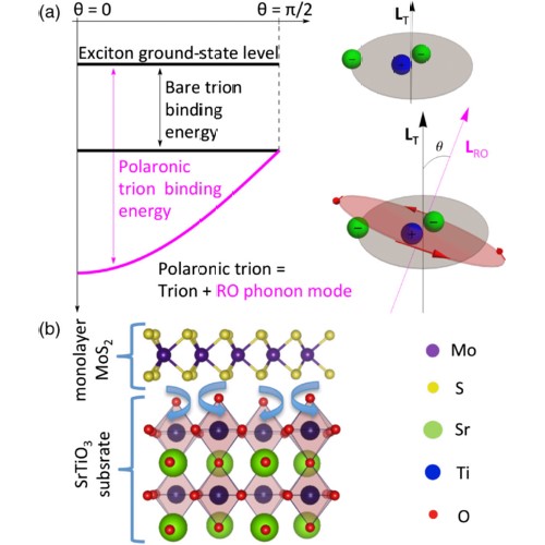 Evidence of Rotational Fröhlich Coupling in Polaronic TrionsElectrons commonly couple through Fröhlich interactions with longitudinal optical phonons to form polarons. However, trions possess a finite angular momentum and should therefore couple instead to rotational optical phonons. This creates a polaronic trion whose binding energy is determined by the crystallographic orientation of the lattice. Here, we demonstrate theoretically within the Fröhlich approach and experimentally by ... | |
M. Trushin et al. ● 20/8/2020 ● Physical Review Letters, 125, 086803 | |
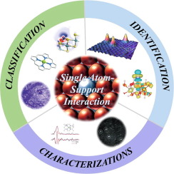 Single atom is not alone: Metal–support interactions in single-atom catalysisSingle-atom catalysts (SACs) have recently attracted interest in the fields of heterogeneous catalysis and electrocatalysis due to the enhancement in intrinsic activity and selectivity through optimized exposure of the active sites. Synthesis of SACs and research into their behavior have helped to elucidate the kinetics and thermodynamics ... | |
K. Qi et al. ● 2/8/2020 ● Materials Today, Volume 40, Pages 173-192 | |
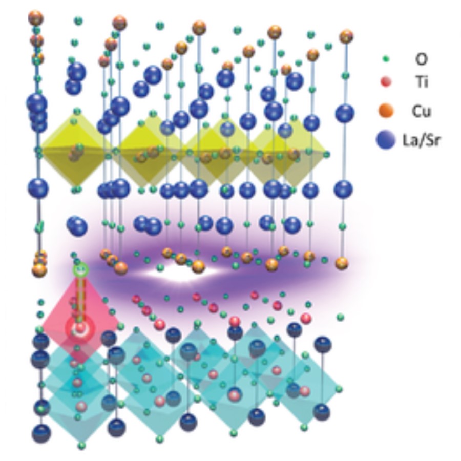 Interfacial Oxygen‐Driven Charge Localization and Plasmon Excitation in Unconventional SuperconductorsCharge localization is critical to the control of charge dynamics in systems such as perovskite solar cells, organic-, and nanostructure-based photovoltaics. However, the precise control of charge localization via electronic transport or defect engineering is challenging due to the complexity in reaction pathways and environmental factors. Here, charge localization in optimal-doped La1.85Sr0.15CuO4 thin-film on SrTiO3 substrate (LSCO/STO) is investigated, and also a high-energy plasmon is observed. Charge localization ... | |
C. S. Tang et al. ● 9/7/2020 ● Advanced Materials, Volume 32, Issue 30 (2000153) | |
 Ultralow-dielectric-constant amorphous boron nitrideDecrease in processing speed due to increased resistance and capacitance delay is a major obstacle for the down-scaling of electronics. Minimizing the dimensions of interconnects (metal wires that connect different electronic components on a chip) is crucial for the miniaturization of devices. Interconnects are isolated from each other by non-conducting (dielectric) layers. So far, research has mostly focused on decreasing the resistance of scaled interconnects because integration ... | |
S. Hong et al. ● 24/6/2020 ● Nature, 582, 511-514 | |
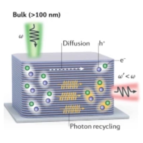 From bulk to molecularly thin hybrid perovskitesOrganic–inorganic hybrid perovskites have been intensively researched in the past decade for their optoelectronic properties. The emergence of Ruddlesden–Popper perovskites, which have mixed dimensionality, has heralded new opportunities for tailor-made semiconductors that combine enhanced stability with useful properties between those of 2D and 3D systems. Inspired by advances ... | |
K.Leng et al. ● 30/3/2020 ● Nature Review Materials, 5, 482-500 | |
 Water-resistant perovskite nanodots enable robust two-photon lasing in aqueous environmentOwing to their large absorption cross-sections and high photoluminescence quantum yields, lead halide perovskite quantum dots (PQDs) are regarded as a promising candidate for various optoelectronics applications. However, easy degradation of PQDs in water and in a humid environment is a critical hindrance for applications. Here we develop a Pb-S bonding approach to synthesize water-resistant perovskite@silica nanodots keeping their emission in water for over six ... | |
S. Li et al. ● 4/3/2020 ● Nature Communications, 11, Article Number 1192 | |
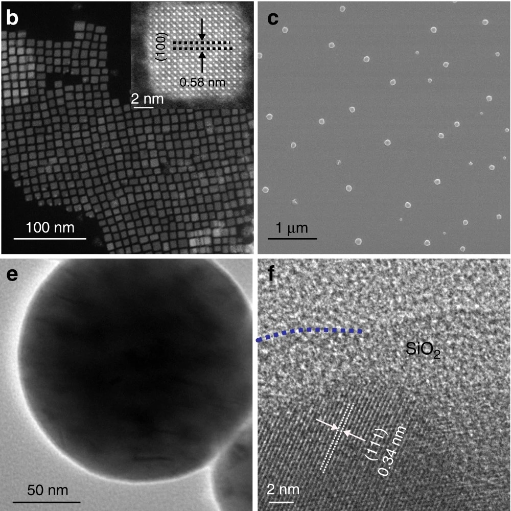
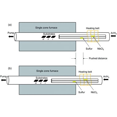 Synthesis of Metallic Mixed 3R and 2H Nb1+xS2 Nanoflakes by Chemical Vapor DepositionIn this work, we report the synthesis and characterization of mixed phase Nb1+xS2 nanoflakes prepared by chemical vapor deposition. The as-grown samples show a high density of flakes (thickness ∼50 nm) that form a continuous film. Raman and X-ray diffraction data show that the samples consist of both 2H and 3R phases, with the 2H phase containing a high ... | |
A. R. Mohmad et al. ● 23/1/2020 ● Faraday Discussions, Volume 227, 2021 | |
| |